Forum rules
The DIY forum is for personal projects (things that are not for sale, not in production), info sharing, peer to peer assistance. No backdoor spamming (DIY posts that are actually advertisements for your business). No clones of in-production pedals. If you have concerns or questions, feel free to PM admin. Thanks so much!
I'm interested in making a bit crushing pedal but haven't found any schematics online.
I'm looking for either the ICs involved in changing the sampling rate or other methods to produce a crushed sample.
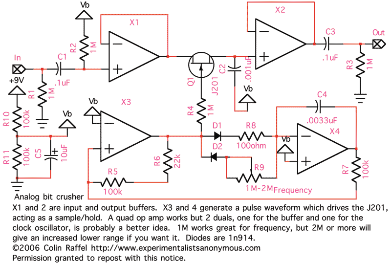
Unfortunately this isn't really a bitcrusher. it's a samplerate reducer, which is one feature of most bitcrushers, but there are no bits to crush in this one. none of that harsh digital clipping and shaping.
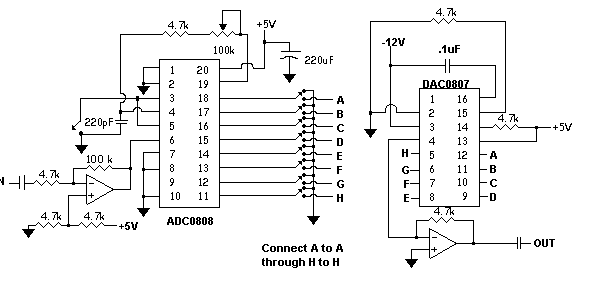
the ADC/DAC method is the only sensible way to make one, without going the microcontroller route. something like this:
this is a true 8bit bitcrusher. bits can be dropped using those toggles and you get awesome noise! I believe the pot at the top-left is samplerate control.
wow nice design. it has a clock made from some inverting logic on the ADC IC. also I noticed you have a single supply for that ADC. this is why ADC0808 is better than ADC0800 for a guitar pedal. I read the datasheet to the DAC0800 and DAC0808,0807,0806. you can definitely do this on a 9.5v single supply. you do not need -12v like that schematic. you just need to understand how to set the Vref- and Vref+. it should be 0v and 5v/2 to interface the ADC0808. you can replace all those 8 switches with a 8 channel OR logic and a pot connected to another ADC0808. this will freeze bits high as you start to turn the pot (control voltage) up at the second ADC.
Thanks for the insights! Just out of curiosity - as I'm going to want to learn how to manually code out some effect eventually - where would be a good place to start to learn how to code effects? I've found massive books on DSP, but maybe something more friendly to the beginner. Thanks again for the help! Can't wait to make these.
read and understand the datasheet for the DAC0808. reading datasheets is a valuable skill. now is your chance to practice your diy skills in a real world situation. on the front page it says +/-4.5v supply. in all the examples it has Vcc pulled up to V+ , Vee to V- and GND somewhere in between. there are also two different DAC0808. national instruments one is in DIP16 and TI one is in DIP28. a little history here---> when chips were made of bipolar junction transistors the power supply was the collector and the emitter. C and E. thats why Vcc and Vee. nothing can be above Vcc or lower than Vee. the standard practice was to use GND 0v as a predetermined level for logic level low and Vcc for logic level high. this also explains why CMOS IC are Vdd and Vss. look up FET for that one. when you interface a chip that has a +5v,0v single supply such as the ADC0808, your logic levels are 0v and +5v (not a surprise?). the datasheet for the DAC0808 will tell you if you logic level high is fixed or adjustable. you can also see if it is possible to use DAC0808 Vee levels (logic low from the ADC0808) for logic low in the DAC0808. without adjustable low and high references on the DAC0808, my single supply plan for everything may actually present a problem of needing logic levels being shifted by some man in the middle device.
Last edited by eatyourguitar on Mon Nov 03, 2014 8:53 pm, edited 1 time in total.
DAC0808 is split supply +4.5v, 0v -4.5v. you need a 10k + 10k voltage divider between 9v and 0v to make the fake ground (fake 0v) where the resistors meet. 9v is your new V+ and old 0v is your new V-. this is a cheap hack for +/-4.5v bipolar supply. you can add a cap from the middle rail to the bottom rail for cleaner power rails. 10uf is good.
if you use this adc you dont need a special "dac" chip. You can just use an opamp as a weighted summation circuit because the ADC has latching outputs and doesn't put garbage on the outputs when preparing the data (weights are 2^0 * R for the MSB then 2^1 * R, 2^2 *R .... 2^7 * R for the LSB, R is some value you choose). This way you can avoid all your power supply troubles. You could even just use a passive R2R ladder,but in the end you will likely want to buffer its output so... Either way it will give you essentially the same result as using this DAC chip at a lower cost and less hassle.
For whatever reason an mcu is frowned on in this thread but in the end an 8 pin mcu is a much nicer solution and use a pwm output. Less parts, lower cos, up 10 bit res most likely as well.
mjmostachetti, I agree with the simpler solution of using an ADC and a DAC to do the required signal clipping and sampling. It is a simple yet elegant solution to your problem. However,someone mentioned using an 8bit MCU in this thread and I can’t say that I disagree to that. You might have to do some smart programming but using a simple MCU can do the job for you without having to go through the ordeal of setting up and a ADC and a DAC.


